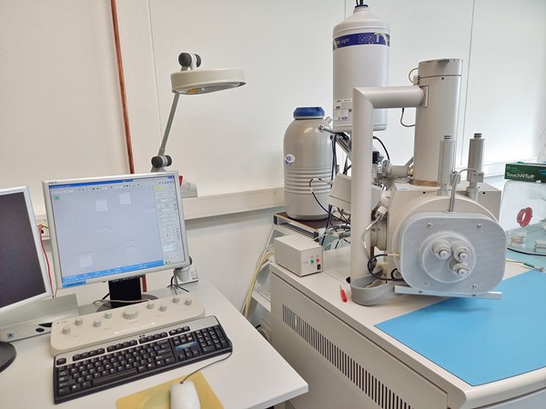
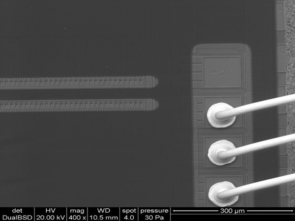
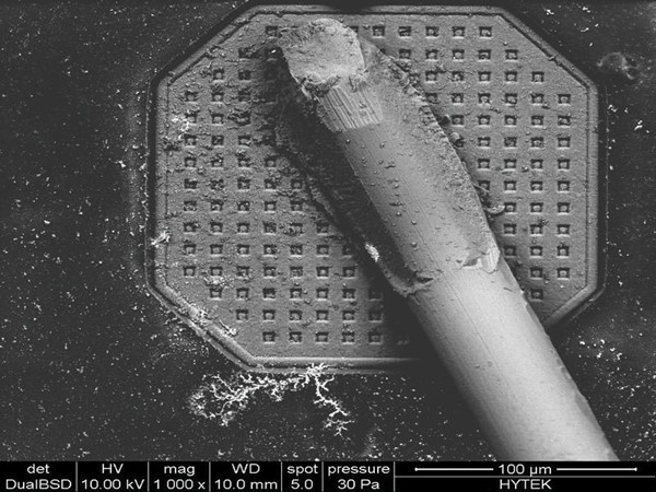
Scanning Electron microscopy/ESEM (Environmental Scanning Electron Microscopy) is a very accurate analytical method that can be used for non-destructive inspection of surfaces at very high magnification. The increasing complexity and higher requirements for reliability place great demands on the inspection equipment. Contrary to ordinary microscopy (see Microscopy inspection), ESEM can be used for topographical inspection even at very high magnification (>X20,000)
The equipment can also be used for elemental identification and calculation of material elements (see Energy dispersive X-ray analysis (EDX).
ESEM can, for example, be used for examination and analysis of:


 3 ?
3 ?