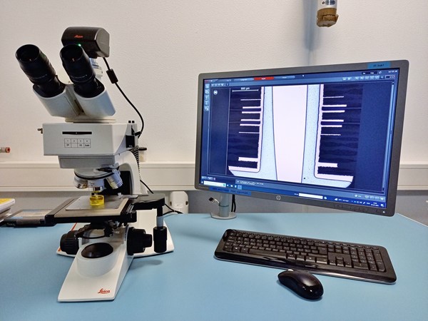
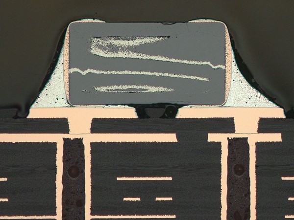
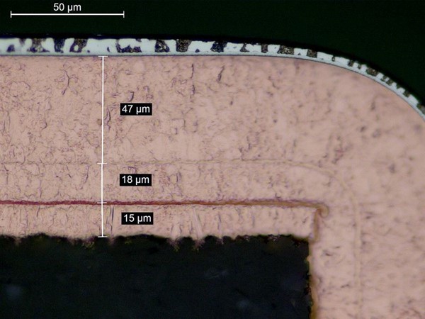
Microscopy inspection is used for examination of items. During a microscopy inspection, you are able to enlarge details while moving or turning the item to get a possibility to investigate the item from different angles. While documenting the microscope has the possibility to look at the item in different magnifications in order to give a closer view of for instance a crack or something else that can be hard to detect with the naked eye.
HYTEK possesses many different microscopes, which all have cameras installed, to document relevant issues during inspection. The microscopes at HYTEK’s laboratory also have the possibilities to look at the item, using different light options (Bright Field, Back-light and Flour cense), in order to improve the recognition of e.g. small cracks or delamination in materials.
Microscopy can, for example, be used for examination and analysis of:

 4 ?
4 ?