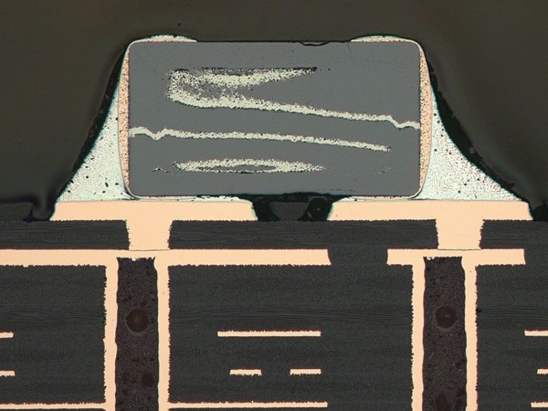
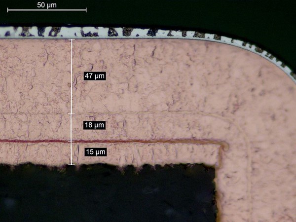
Microsectioning preparation is a method that is used if sub-elements are to be examined ingreat detail and accurately internally in materials, for example in componentsor printed circuit boards (PCB). Microsectioning is a very effective method formetallographically inspection, characterizing or analyzing of encapsulated/hiddenelements, e.g. in solder joints, including analysis of potential failuremechanisms.
HYTEK is recognizedby the European Space Agency ESA as a recommended supplier of microsectioningto the space industry (ESA memo ESA-TECMSP-MO-013165 issue 1: ESA recommendedmicrosectioning facilities).
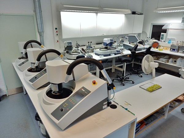
HYTEK has avery advanced line for microsectioning, consisting of 4 semi-automatic grindingmachines followed by 3 semi-automatic polishing machines.
Microsectioning can, for example, be used for examination and analysis of:


 4 ?
4 ?